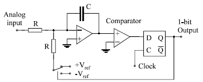
Fig. 5.34: First order sigma-delta modulator.
The oversampling sigma-delta conversion technique offers an alternative method of producing high-accuracy, high-resolution ADC’s without the need for precise component matching and complex analog circuitry.
Fig. 5.34: First order sigma-delta modulator.
A first order sigma-delta modulator is shown in Fig. 5.34. The gain of the circuit is given by
which means that it is dependent on the sampling rate. If the primary gain is designed for the lowest sampling rate, the gain will decrease with increasing sampling rate, reducing the dynamic range of the modulator.
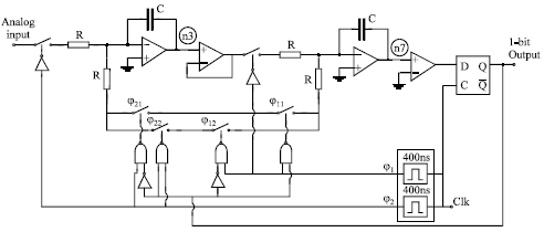
A way to keep the gain constant is to make the integrator charging time invariable with respect to clock rate. This means that the analog switch must be turned on for fixed time duration regardless of clock rate. One solution for achieving this is to use monostable multivibrator as a fixed-width pulse generator in the circuit. A second order sigma-delta modulator with variable sampling rate is shown in Fig. 5.35.
The monostable multivibrator between the clock input and switch control block functions as a pulse generator to produce control signals of fixed time duration. The pulse width is chosen such that the circuit operates at the maximum clock rate of 1.024 MHz. The reference voltages of this circuit are ±1.5 V.
Fig. 5.35: Second order sigma-delta modulator.
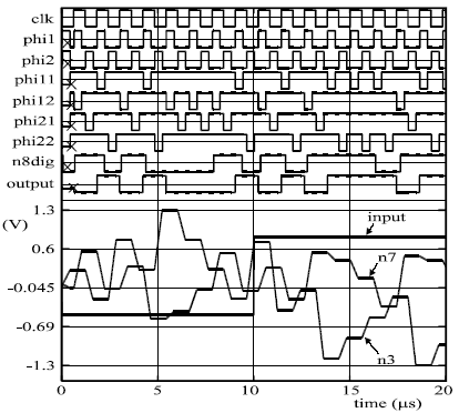
Fig. 5.36: Simulation results of sigma-delta modulator with two-level input excitation.
Results of the simulation, when two levels of a constant analog signal are brought to input, are given in Fig. 5.36. All digital signals in the circuit, and three analog signals (input, and two voltages at the output of the integrators) are plotted out.
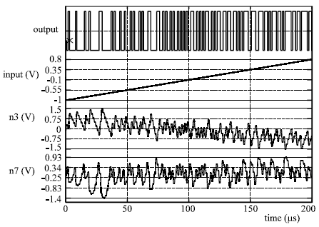
Fig. 5.37 shows reaction of the system when the input is excited by a linear ramp. The simulation time is longer, and the changes of the output can be noticed.
Fig 5.37: Simulation results for linear ramp excitation